李亚飞教授课题组在JOURNAL OF MATERIALS CHEMISTRY C发表研究论文
Pd2Se3 monolayer: a novel two-dimensional material with excellent electronic, transport, and optical properties
Zhu, XR (Zhu, Xiaorong)[ 1 ] ; Li, F (Li, Feng)[ 1 ] ; Wang, Y (Wang, Yu)[ 1 ] ; Qiao, M (Qiao, Man)[ 1 ] ; Li, YF (Li, Yafei)[ 1 ]*(李亚飞)
[ 1 ] Nanjing Normal Univ, Sch Chem & Mat Sci, Jiangsu Collaborat Innovat Ctr Biomed Funct Mat, Jiangsu Key Lab New Power Batteries, Nanjing 210023, Jiangsu, Peoples R China
JOURNAL OF MATERIALS CHEMISTRY C,201804,6(16), 4494-4500
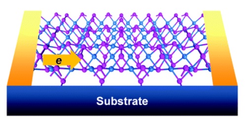
Two-dimensional (2D) crystals of atomic thickness with a band gap in the range of 0.3-1.5 eV, which corresponds to the solar spectrum range from mid-infrared to near-infrared and matches that of commercial silicon and III-V semiconductor materials, are highly sought for future electronic and optoelectronic technologies. In this study, by means of comprehensive density functional theory computations, we demonstrated that the recently synthesized 2D Pd2Se3 monolayer is a promising candidate. According to our computational results, Pd2Se3 monolayer is a semiconducting material with a moderate band gap of 0.45 eV and its carrier mobility (178.02 cm(2) V-1 s(-1)) is comparable to that of the MoS2 monolayer. In particular, Pd2Se3 monolayer exhibits novel anisotropic transport properties and has a rather good current-voltage character. Moreover, Pd2Se3 monolayer shows a very pronounced optical absorption that covers almost the entire solar spectrum. With these excellent properties, Pd2Se3 monolayer would have wide applications in electronic and optoelectronic devices.
文章链接:
http://pubs.rsc.org/en/Content/ArticleLanding/2018/TC/C8TC00810H#!divAbstract
版权与免责声明:本网页的内容由收集互联网上公开发布的信息整理获得。目的在于传递信息及分享,并不意味着赞同其观点或证实其真实性,也不构成其他建议。仅提供交流平台,不为其版权负责。如涉及侵权,请联系我们及时修改或删除。邮箱:sales@allpeptide.com